• Skip to WISTA Sites
  • Skip to Main menu
  • Skip to Page content
WISTA Logo
  • WISTA
  • WISTA.Plan
  • WISTA.Service
  • Adlershof
  • Charlottenburg
  • South West
  • Marzahn
WISTA direkt
Search
  • de
  • en
  • WISTA Logo
  • About
    • Mission / Management
      • Company Profile
      • Team
      • Boards
      • Annual Reports
      • Invitations to tender
    • Sustainability / Diversity
    • Subsidiaries
    • Directions
  • News / Press
    • Overview
    • News
    • Events / Calendar
      • Diversity Conference Adlershof
    • Social Media Wall
    • Press
    • Magazine "Potenzial"
    • Adlershof Journal
    • Downloads
  • Services
    • All WISTA services
    • Business programmes
      • Adlershof Founder's Lab
    • Networks / Cooperations
    • Talent promotion / Recruiting
    • Event and Visitors Service
  • Projects
    • Focus Topics
    • Team Innovation
  • Sites
    • Overview
    • Technology Park Adlershof
    • Innovation Centre CHIC Charlottenburg
    • Innovation Campus FUBIC South West
    • CleanTech Business Park Marzahn
    • Business Office “Zukunftsorte”
  • Real Estate
    • Current Real Estate Offers
    • ST3AM Working Environments
    • Facility Management
  • Talents
    • Overview
    • WISTA as Employer
      • Jobs
    • WISTA Academy
      • Overview
    • Talent Promotion / Training
  • WISTA
  • WISTA.Plan
  • WISTA.Service
  • Adlershof
  • Charlottenburg
  • South West
  • Marzahn
WISTA direkt

News / Press

  • Overview
  • News
  • Events / Calendar
  • Social Media Wall
  • Press
  • Magazine "Potenzial"
  • Adlershof Journal
  • Downloads
  • Editorial Staff
  • WISTA
  • News / Press
12. August 2024

IKZ, BAM, UDE and BESTEC successfully completed KostSol project

The aim of the joint project was to reduce costs in the production of Cu(In,Ga)Se2 solar cells through laser-induced structure formation on surfaces

Indium-Array
Indium array produced through thermal decomposition of trimethylindium using laser radiation Credit: ©IKZ

The joint project "Cost-Efficient Fabrication of Cu(In,Ga)Se2 Solar Cells through Laser-Induced Surface Structuring" (KostSol), funded by the Federal Ministry of Economics and Climate Protection (BMWK), in co-operation with the Federal Institute for Materials Research and Testing (BAM), the University of Duisburg/Essen (UDE) and the industrial partner BESTEC GmbH, has been successfully completed.

The approach of using laser radiation to grow patterned crystalline structures on amorphous surfaces, thereby replacing complex masks or lithography techniques, has been successfully realized.

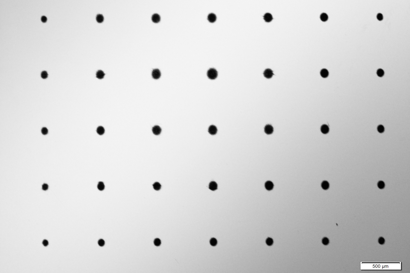
For this purpose, laser radiation with a specific wavelength and intensity was employed and directed through a diffractive optical element (DOE), creating a patterned thermal inhomogeneity on the target substrate.

Thermal decomposition of organometallic gases at elevated temperatures was used to selectively form liquid and, subsequently crystalline island-shaped structures on the surface. Using this method, CuInSe2 islands in the micrometer range were fabricated and processed into micro-concentrator solar cells.

For this project, a PVD-CVD cluster system (physical vapor deposition and chemical vapor deposition) with an integrated laser system has been developed and tested. The locally selective deposition of the localized structures in the micrometer range can be used for a variety of other applications, particularly in semiconductor industry.

The project partners IKZ, BAM, UDE and the company BESTEC, as well as the contractors Mergenthaler GmbH, CSE GmbH and the Fraunhofer Heinrich Hertz Institute Berlin worked closely together to realize the project.


Contact:

Leibniz-Institut für Kristallzüchtung (IKZ)
Dr. Setareh Zahedi-Azad
+49 30 6392-2852
setareh.zahedi-azad(at)ikz-berlin.de

Dr. Torsten Boeck
+49 30 6392-3051
torsten-boeck(at)ikz-berlin.de


Press release of IKZ 08.08.2024.

Research Microsystems / Materials Photonics / Optics Renewable Energies

Related News

  • Schematic illustration of the novel Raman spectroscopy technique © Heeg/HU Berlin

    Novel Raman spectroscopy technique for investigation of thin films and surfaces

    Enhanced surface-to-bulk Raman signal ratio using a transferable porous gold membrane
  • Photograph of an investigated Si crystal © IKZ

    IKZ and Bruker Nano demonstrate a new X-ray topography method

    Non-destructive, high-throughput identification of defects in high-quality single crystals can be facilitated
  • IKZ-employees in front of of an image of a BaMgF4 crystal grown at IKZ

    Successful start of the BMBF project "UV-KrisP - Coherent continuous wave radiation in vacuum UV"

    IKZ and Fraunhofer IPM will develop a new crystal material together

Related Institutions

  • Leibniz-Institut für Kristallzüchtung im Forschungsverbund Berlin e.V. (IKZ)
  • BAM Bundesanstalt für Materialforschung und -prüfung
  • BESTEC GmbH
  • LinkedInshare0
  • Facebookshare0
  • WhatsAppshare0
  • E-Mail
  • © WISTA Management GmbH
  • Legal Notice
  • Privacy Policy
  • Contact
  • Career
  • Press
  • Social Media Guide
Member of:
Zukunftsorte Logo