• Skip to WISTA Sites
  • Skip to Main menu
  • Skip to Page content
WISTA Logo
  • WISTA
  • WISTA.Plan
  • WISTA.Service
  • Adlershof
  • Charlottenburg
  • South West
  • Marzahn
WISTA direkt
Search
  • de
  • en
  • WISTA Logo
  • About
    • Mission / Management
      • Company Profile
      • Team
      • Boards
      • Annual Reports
      • Invitations to tender
    • Sustainability / Diversity
    • Subsidiaries
    • Directions
  • News / Press
    • Overview
    • News
    • Events / Calendar
      • Diversity Conference Adlershof
    • Social Media Wall
    • Press
    • Magazine "Potenzial"
    • Adlershof Journal
    • Downloads
  • Services
    • All WISTA services
    • Business programmes
      • Adlershof Founder's Lab
    • Networks / Cooperations
    • Talent promotion / Recruiting
    • Event and Visitors Service
  • Projects
    • Focus Topics
    • Team Innovation
  • Sites
    • Overview
    • Technology Park Adlershof
    • Innovation Centre CHIC Charlottenburg
    • Innovation Campus FUBIC South West
    • CleanTech Business Park Marzahn
    • Business Office “Zukunftsorte”
  • Real Estate
    • Current Real Estate Offers
    • ST3AM Working Environments
    • Facility Management
  • Talents
    • Overview
    • WISTA as Employer
      • Jobs
    • WISTA Academy
      • Overview
    • Talent Promotion / Training
  • WISTA
  • WISTA.Plan
  • WISTA.Service
  • Adlershof
  • Charlottenburg
  • South West
  • Marzahn
WISTA direkt

News / Press

  • Overview
  • News
  • Events / Calendar
  • Social Media Wall
  • Press
  • Magazine "Potenzial"
  • Adlershof Journal
  • Downloads
  • Editorial Staff
  • WISTA
  • News / Press
10. June 2024

IKZ and Bruker Nano demonstrate a new X-ray topography method

Non-destructive, high-throughput identification of defects in high-quality single crystals can be facilitated

Photograph of an investigated Si crystal © IKZ
Photograph of an investigated Si crystal with a similar viewing direction like the X-ray beam (b) superimposed greyscale-coded 2D intensity plot of peak flanks and peak maxima of the 337 and 448 reflections with a slight increase of contrast (Rh source with AMS) of the sample shown in (a). © IKZ

The IKZ in cooperation with Bruker Nano GmbH, Berlin, demonstrate that high-resolution energy-dispersive X-ray fluorescence mapping devices based on a micro focused beam are not restricted to high-speed analyses of element distributions or to the detection of different grains, twins and subgrains in crystalline materials, but can also be used for the detection of dislocations in high quality single crystals.

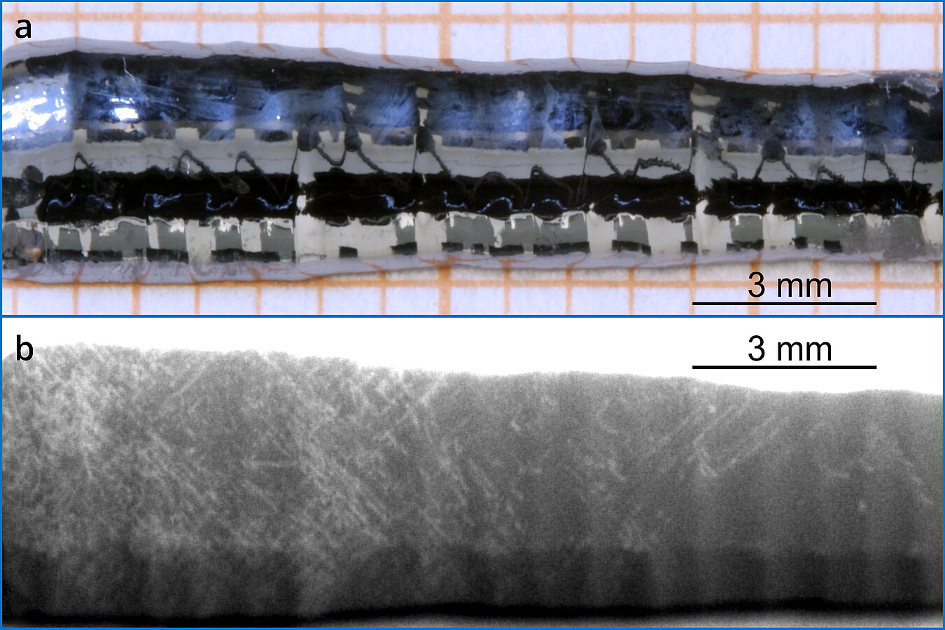
Si single crystals with low dislocation densities were used as model materials to visualize the position of dislocations by the spatially resolved measurement of Bragg peak intensity fluctuations. These originate from the most distorted planes caused by the stress fields of dislocations. Moreover, the beam divergence was reduced via an Aperture Management System (AMS) to facilitate the visualization of dislocations for virtually as-grown, non-polished and non-planar samples with a very pronounced surface profile. While non-planar surfaces distort the wave field in standard XRT techniques due to an inhomogeneous phase-shift that is a consequence of surface height variations, this is not a critical issue for the presented energy-dispersive scanning technique, since it is realized by scanning with a focused, convergent beam.

Based on the widespread availability of µ XRF devices, the described methodology can facilitate the non-destructive, high-throughput identification of defects in high-quality single crystals.

Publication:

Application of laboratory micro X-ray fluorescence devices for X-ray topography
C. Guguschev, C. Hirschle, K. Dadzis, A. Kwasniewski, M. Schulze, L. Schellkopf and C. Richter (2024).
J. Appl. Cryst. 57, 734-740, doi.org/10.1107/S1600576724003509

Contact:

Leibniz-Institut für Kristallzüchtung (IKZ)
Max-Born-Straße 2, 12489 Berlin
www.ikz-berlin.de

Dr. Christo Guguschev
christo.guguschev(at)ikz-berlin.de

Dr. Carsten Richter
carsten.richter(at)ikz-berlin.de


Bruker Nano GmbH
Am Studio 2D, 12489 Berlin
Dr. Christian Hirschle
christian.hirschle(at)bruker.com
www.bruker.com/nano-analytics


Press release IKZ, 7 June 2024

Research Analytics Photonics / Optics

Related Institutions

  • Bruker Nano GmbH
  • Leibniz-Institut für Kristallzüchtung im Forschungsverbund Berlin e.V. (IKZ)
  • LinkedInshare0
  • Facebookshare0
  • WhatsAppshare0
  • E-Mail
  • © WISTA Management GmbH
  • Legal Notice
  • Privacy Policy
  • Contact
  • Career
  • Press
  • Social Media Guide
Member of:
Zukunftsorte Logo