Tailor-made crystals
The IKZ develops indispensable raw materials for the high-tech industry
Crystals are most commonly associated with glistening chandeliers or the spheres of fortune tellers. However, the lattice structures have become indispensable raw materials for the high-tech industry.
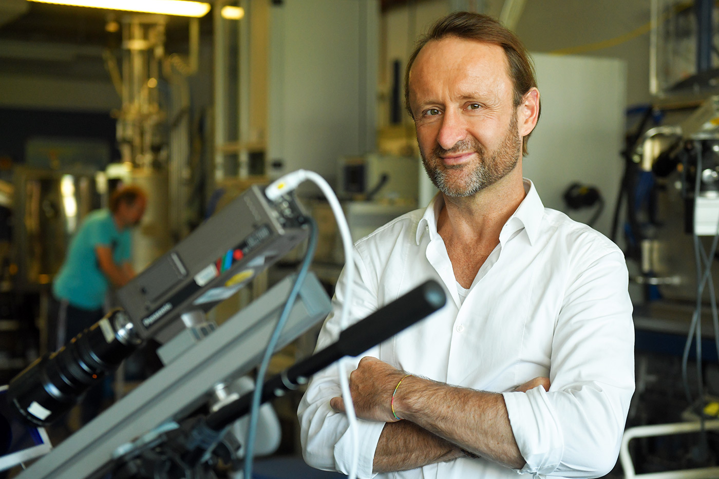
The regular, repeating structure of a crystal lattice follows the laws of nature. “The structure is the result of a phase transition. The components – most often, atoms – reach a higher packing density and thus a more stable state,” says Thomas Schröder, who is a professor for crystal growth Humboldt-Universität zu Berlin. He became the director of the IKZ Leibniz Institute for Crystal Growth in Adlershof in February 2018.
However, the lattice is not always perfect. Gaps as well as foreign atoms , including contamination, and other mechanisms can lead to defects, says Schröder, who graduated in physics and chemistry. Such deficiencies are intolerable for high-performance materials used in electronics, optics or energy technology. In fact, the raw materials required today, which include silicones, germanium, gallium arsenide, aluminium nitride, aluminium oxide, and fluoride crystals, have optimised properties geared towards a specific type of application. Such tailor-made crystals do not occur naturally. Growing them is a complex process that requires much expertise. The refinement of these growing methods, including growing them from a melt, growing them from a solution, or through chemical vapor deposition, is the mission of the 120 employes of the IKZ, which is one of the leading institutes in its field.
Schröder demonstrates the path from the raw material to the computer chip. The materials researcher shakes a bottle of sand and puts it on the table. There is a round silicone monocrystal next to it that is made from said sand. It is about ten centimetres thick and 20 cm long. An ultrathin, glittering disc, a so-called wafer, is lying next to it. It serves as a ‘substrate’, a foundation for electronic components. IKZ supplies research institutes and companies with this crystal substrate for producing semiconductor chip systems. Nowadays, crystals are the basis for lasers, solar cells as well as everyday appliances like smartphones, computers, and navigation systems, devices that Schröder likes to call the “cultural heritage of the 21st century.”
In recent decades, the motto for developing these products was: let’s fit more chips in increasingly less space. According to Schröder, this development is slowly coming to end due to the excessive costs required to attain the necessary precision. Researchers and companies in need of a growth strategy could lean towards integrating new modules, including biological functions, into tried-and-tested technologies like radio, photography, and the internet. This will require new materials. This is an opportunity for the IKZ to go beyond successful crystal growth towards developing innovative crystal substances for research facilities and companies.
Such yet-to-be established raw materials with enormous market potential, such as quantum materials, often lack industrial-scale suppliers, says Schröder. The Saarland-native learned interdisciplinary cooperation from scratch. After his double degree in Tübingen and a range trips to other countries, including in Italy, Spain and France, he was a researcher at the Leibniz Institute for Innovative Microelectronics in Frankfurt/Oder, most recently as head of the department Materials Research before he was called to Berlin.
By Paul Janositz for Adlershof Journal