Organic electronics: a novel semiconductor from the family of carbon nitrides
Research teams from HU and HZB have investigated a triazine-based graphitic carbon nitride that is useful in optoelectronic applications
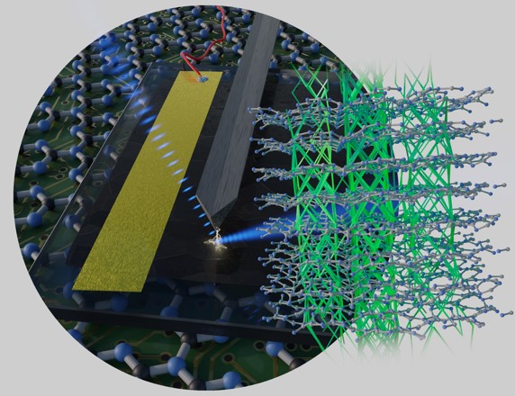
Research teams from the Humboldt-Universität and the Helmholtz Zentrum Berlin (HZB) have investigated a new material from the family of carbon nitrides. Triazine-based graphitic carbon nitride (TGCN) is a semiconductor that is useful in optoelectronic applications. Its structure is two-dimensional and layered, and it resembles that of graphene. Unlike graphene, its conductivity between the layers is 65-times higher than in-plane.
Some organic materials can be used in optoelectronics just like silicon-based semiconductors. Whether in solar cells, light-emitting diodes, or as transistors – the important property is the bandgap, i.e. the energy-difference of the electrons in the valence band and the conduction band. The basic principle underlying all electronic components is that electrons can be promoted by light or by voltage between the valence and the conduction band. Here, bandgaps between 1 and 2 eV are ideal.
A team led by the chemist Dr. Michael J. Bojdys from the chemistry department and IRIS Adlershof of the Humboldt-Universität zu Berlin, has recently synthesized an organic semiconductor from the family of carbon nitrides. This triazine-based graphitic carbon nitride (TGCN) consists exclusively from carbon and nitrogen atoms and can be grown as a brown film on quartz glass substrates. The C- and N-atoms connect in hexagonal, honeycomb patterns like carbon atoms in graphene. Just like in graphene, the crystal structure of TGCN is based on layered, two-dimensional sheets. In graphene, in-plane conductivity is excellent, however, it is much lower through the planes. In the case of TGCN, the opposite is observed: through-plane conductivity is 65-times higher than in-plane. With a bandgap of 1.7 eV TGCN is a good candidate for optoelectronic applications.
The HZB-physicist Dr. Christoph Merschjann has examined the charge carrier transport in samples of TGCN using time-resolved absorption measurements in the femto- to nanosecond regime at the laser lab JULiq – a joint lab between the HZB and the Freie Universität Berlin. Such laser experiments offer a unique way to correlate macroscopic conductivity and microscopic transport models. From his measurements, he was able to deduce how the charge carriers diffuse throughout the material. “Electrons do not exit the hexagonal honeycombs of triazine units horizontally, but they move at a slope to the nearest triazine-unit in the neighboring layer. The crystal structure of the material leads to a preferred movement of charge carriers along tube-like channels.” This mechanism could explain why the conductivity of TGCN is fundamentally higher through-plane than in-plane.
“TGCN is the hitherto best candidate to replace silicon semiconductors and the critical, rare-earth dopants used in their manufacture”, says Michael Bojdys. “The production method for TGCN that we developed in my group at the Humboldt-Universität zu Berlin yields flat layers of semiconducting TGCN on insulating quartz glass. This enables relatively easy upscaling and device production.”
These results were recently published in the international edition of the renowned journal “Angewandte Chemie” (DOI: 10.1002/anie.201902314).