
Imaging Ellipsometry for Process Control of Thin-Film Devices
The method developed at HZB enables non-destructive characterisation and quality control of microstructured MXene thin films during device fabrication
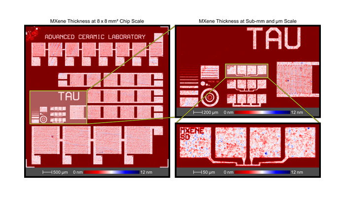
A German–Israeli research team led by Dr. Andreas Furchner has demonstrated how imaging ellipsometry enables non-destructive characterisation and quality control of microstructured MXene thin films during device fabrication. The authors used two complementary ellipsometry approaches for precise, multi-scale access to key material properties. The work positions imaging ellipsometry as a powerful platform for monitoring thin-film uniformity, device integrity, and functionality throughout processing, including critical lithographic steps. The study was published in Applied Physics Letters and selected as an Editor’s Pick.
MXenes are two-dimensional nanomaterials that can serve as building blocks for microscale electronic and photonic devices, often referred to as MXetronics. At Tel Aviv University, structured MXene-based thin films are being investigated as backside electrodes in next-generation photodetectors. Imaging ellipsometry turned out to be a crucial non-destructive technique for monitoring their properties throughout processing without damaging the device.
By analyzing changes in the polarization state of light reflected off the device, ellipsometry provides direct, quantitative access to thin-film characteristics such as thickness, composition, and charge-transport properties. The resulting optical contrast is highly sensitive to even subtle lateral variations across a sample. The method is not only imaging structures but also functionality, which makes ellipsometry valuable for device fabrication.
The authors pursued two optical approaches. Spectroscopic micro-ellipsometry (SME), available at The Hebrew University of Jerusalem, provides high-resolution single-spot measurements that enable rapid probing of samples. SME is well suited for targeted checks and high-throughput assessment during fabrication, giving a fast snapshot of what is happening at a precise point on the device.
Imaging spectroscopic ellipsometry (ISE), by contrast, provides spatially resolved imaging across full thin-film devices. At HZB, a Park Systems imaging ellipsometer is available for large-scale imaging, complemented by a unique focusing optic with lateral resolution down to 1 µm. This enables structural and functional film properties to be mapped across entire devices, effectively connecting millimeter to micrometer length scales in a single comprehensive measurement approach.
A particular strength of the method is its ability to monitor and visualize how local properties evolve during processing steps such as photoresist development. These changes can be tracked through their impact on the optical response, revealing spatial variations in charge-transport and structural properties without contacting the device. Local properties can thereby be correlated with overall device functionality, which is essential for optimization and fabrication.
There is already keen interest in the method, both within HZB and from international research groups, which has led to ongoing collaborations. The highly versatile ellipsometer is suitable for analyzing a wide range of isotropic and anisotropic materials, including two-dimensional systems. The HZB team always welcomes interested researchers to get in touch for measurements or potential collaborations.
Publication:
Applied Physics Letters (2026): Special Topic “Advances in Spectroscopic Ellipsometry Methods and Materials Characterization”. Editor’s Pick: Spectroscopic Imaging- and Micro-Ellipsometry of MXene-Based Microelectronic Devices
Andreas Furchner, Ralfy Kenaz, Bar Favelukis, Maxim Sokol, Ronen Rapaport, and Tristan PetitHZB, The Hebrew University of Jerusalem, Tel Aviv University
DOI: 10.1063/5.0314586
Contact:
Dr. Andreas Furchner
Helmholtz-Zentrum Berlin für Materialien und Energie (HZB)
Young Investigator Group Nanoscale Solid-Liquid Interfaces
(030) 8062-17176
andreas.furchner(at)helmholtz-berlin.de
HZB press release, 22 May 2026