Analytics simplified
Helmholtz and BAM scientists show alternative method for the representation of microstructures in polycrystalline materials
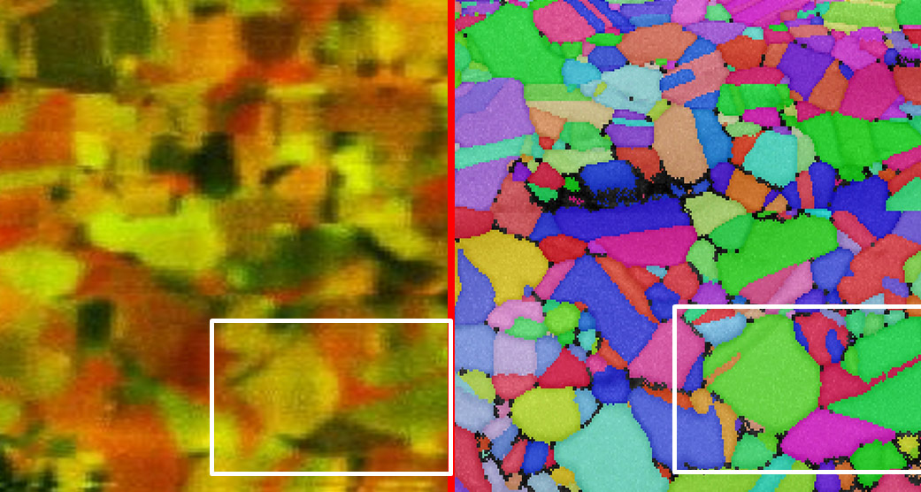
Also Raman microspectroscopy in an optical microscope provides the means to determine local crystal orientations of polycrystalline materials over large sample areas. This method can be used alternatively to electron backscatter diffraction in a scanning electron microscope. It was shown by a team from Helmholtz-Zentrum Berlin and the Federal Institute for Materials Research and Testing (BAM) that both characterization techniques result in similar orientation distribution maps on areas of several hundreds of square micrometers.
Most solid materials are of polycrystalline nature. In which way the individual grains are oriented in the material can be relevant for its functional properties. In order to determine the corresponding orientation distributions on large specimen areas, generally, a scanning electron microscope is employed. The specimen surface needs to be prepared, before it can be probed under vacuum by an electron beam and analyzed using electron backscatter diffraction (EBSD).
It has now been shown by a team at HZB headed by Dr. Daniel Abou-Ras, together with Dr. Thomas Schmid from BAM, that equivalent orientation distribution maps can be obtained also by means of Raman microspectroscopy. This method needs only an optical microscopy setup, no time-consuming specimen preparation, and can also be conducted under ambient conditions.
The scientists used CuInSe2 thin films as a model system for their study. They showed that the experimental Raman intensities correspond well with the theoretical intensities calculated by using the local orientations from the EBSD map. “The sample area was scanned by a laser beam using step sizes of 200 nanometers. For such measurement conditions, the sample environment needs to be controlled carefully and kept stable for several hours,” explains Dr. Abou-Ras.
The application of Raman microspectroscopy for orientation distribution analysis is possible in principle for all polycrystalline materials, whether they are inorganic or organic, as long as they are Raman active.
The report has been published in Scientific Reports:
Orientation-distribution mapping of polycrystalline materials by Raman microspectroscopy, Norbert Schäfer, Sergiu Levcenco, Daniel Abou-Ras, Thomas Schmid Doi: 10.1038/srep18410
More information:
Helmholtz-Zentrum Berlin für Materialien und Energie
Institute Nano-architectures for Energy Conversion
Priv.-Doz. Dr. Daniel Abou-Ras
Tel.: (030) 8062-43218
Norbert Schäfer
Tel.: (030) 8062-43231
EM-ASD-office(at)helmholtz-berlin.de
Federal Institute for Materials Research and Testing
Thomas Schmid